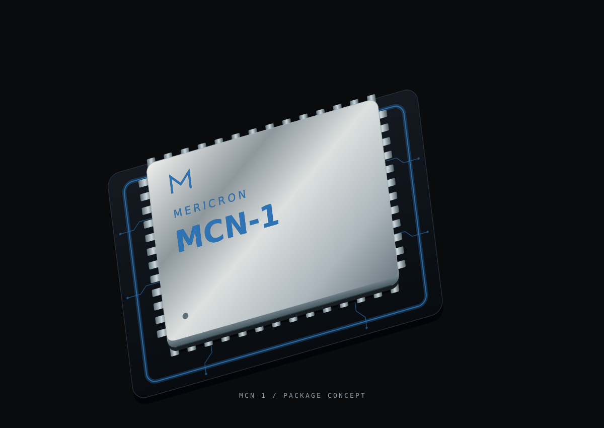
MCN-1
A pre-silicon, two-die wireless microcontroller system-in-package. The compute die carries the application and security cores. The radio die carries a 400 MHz RISC-V baseband core, dual-band Wi-Fi 6, Bluetooth 5.4 LE, and the RF Compliance Firewall.
2 application cores · QFN-56, 7 × 7 mm
Two application cores
The MCN-1 uses two 400 MHz RV32 application cores. A separate always-on security core runs at 100 MHz and can burst to 400 MHz for post-quantum operations.
Owner controlled root of trust
Customers can use their own secure-boot keys instead of relying on Mericron to authorize firmware. Hybrid secure boot, measured boot, attestation, and rollback protection remain available.
Dedicated 400 MHz radio core
A 400 MHz RV32 baseband core with 256 KB SRAM runs the open Wi-Fi 6 MAC and Bluetooth 5.4 LE controller.
CPU subsystem
The FPGA prototype demonstrates concurrent security, application, and radio domains with bus-level access isolation at 50 MHz. PMP/ePMP, world-ID tagging, and IOPMP remain production-silicon enforcement targets.
| Application cores | 2× 32-bit RISC-V |
|---|---|
| Application core frequency | 400 MHz (max) |
| Security core | 1× 32-bit RISC-V, always-on island |
| Security core frequency | 100 MHz island; up to 400 MHz burst for PQC operations |
| Radio baseband core | 1× RV32IMC at 400 MHz on the radio die |
| Application pipeline | 4-stage, in-order |
| Radio-core memory | 256 KB SRAM, no cache |
| ISA extensions | Application: I, M, A, C, B, Zkn/Zks; security and radio: RV32IMC-class |
| Memory protection | PMP / Enhanced PMP (Smepmp) |
| DMA isolation | IOPMP on all DMA-capable masters |
| Interrupt controller | RISC-V CLIC |
| Debug | JTAG/SWD with owner-controlled debug authentication |
Memory
| Region | Size | Notes |
|---|---|---|
| Boot ROM | 64 KB | Immutable mask ROM with published source and build recipe |
| Secure SRAM | 64 KB | Security-core only; parity and scrub |
| Main SRAM | 768 KB | PMP/IOPMP-partitioned |
| L1 cache (per app core) | 16 KB instruction + 16 KB data | Software-managed coherency model |
| Radio SRAM | 256 KB | Code and packet buffers on D2 |
| In-package flash (option) | 8 / 16 MB | AES-XTS; package feasibility pending |
| eFuse / OTP | 8 KB on D1 | Owner/vendor keys, anti-rollback counters, and SKU configuration |
| Regulatory eFuse | D2-local | Regulatory key and anti-rollback state; not writable by D1 |
Security subsystem
Root-of-trust and physical-hardening entries describe production silicon. FPGA-demonstrated boot, measurement, and attestation results are identified separately.
| Device identity | PUF; implementation choice is deferred to the test chip |
|---|---|
| Entropy source | TRNG per NIST SP 800-90B with continuous health tests |
| Key storage | 8 KB D1 OTP plus 64 KB security-core SRAM |
| Boot ROM | 64 KB immutable mask ROM with deterministic published build |
| Boot chain | Multi-stage, ROM-anchored |
|---|---|
| Bootloader signature | Ed25519 + ML-DSA-87 hybrid; both must verify |
| Firmware authority | Owner root-key enrollment with Mericron firmware authority revocable by the owner |
| Measurement | SHA-3-384 extended into on-die PCRs |
| Anti-rollback | Monotonic OTP counters |
| Attestation | Security-core-signed quote over SHA3-384 PCR measurements |
DPA / EM countermeasures
Masked AES and lattice-cryptography datapaths, security-island clock controls, and an active shield over key registers and the PUF.
Glitch protection
Voltage-glitch detector, clock-integrity monitor, redundant secure-boot decision logic, and a dual-redundant secure-boot decoder.
Physical hardening
Bus scrambling, key-whitened secure SRAM, and an active top-metal shield, subject to 22FDX implementation feasibility.
Cryptographic accelerators
Target production services from the always-on security subsystem. Ed25519 and ML-DSA-87 verification plus SHA3-384 measured boot have been proven in the hardware prototype.
| Algorithm | Target implementation | Standard |
|---|---|---|
| AES-256 (GCM/XTS) | DPA-masked hardware path | FIPS 197 |
| SHA-2 / SHA-3 | Hardware-backed hashing and measured boot | FIPS 180-4 / 202 |
| HMAC + HKDF | Security-core service | RFC 2104 / 5869 |
| ECDSA P-384 | Classical signature service | FIPS 186-5 |
| Ed25519 / X25519 | Classical signature and key-agreement service | RFC 8032 / 7748 |
| ML-KEM-1024 | Planned masked NTT accelerator | FIPS 203 |
| ML-DSA-87 | Masked accelerator planned for silicon; firmware verification demonstrated on FPGA | FIPS 204 |
| SLH-DSA | Firmware fallback | FIPS 205 |
| TRNG | Continuous health tests; production raw access disabled | SP 800-90B |
Wireless / RF subsystem
This section describes intended production silicon. Integrated RF and the open Wi-Fi/Bluetooth firmware stack have not been demonstrated in the FPGA prototype.
| Standard | IEEE 802.11ax (Wi-Fi 6); 802.11a/b/g/n/ac compatible |
|---|---|
| Topology | 1×1 single-stream |
| Bands | 2.4 GHz + 5 GHz (dual-band) |
| Key 802.11ax features | OFDMA, TWT (Target Wake Time), BSS coloring |
| Security | WPA3 |
| Front-end | On-die PA, LNA, and switch |
| 2.4 GHz Tx power | +20 dBm (on-die) |
| 5 GHz Tx power | +16 dBm (on-die) |
| Firmware | Open upper/lower MAC and PHY-control firmware; no opaque runtime blobs |
| Version | Bluetooth 5.4 LE |
|---|---|
| LE features | 1M/2M/coded PHY, extended advertising, PAwR, and EAD |
| Coexistence | Documented on-die PTA with firmware-visible priority controls |
Peripherals & I/O
| Interface | Quantity | Notes |
|---|---|---|
| GPIO | 38 | Secure-world-lockable bits |
| UART | 4 | — |
| SPI | 3 | 1× octal-capable high-speed interface |
| I²C | 2 | — |
| I²S | 2 | — |
| CAN-FD | 2 | External transceivers required |
| USB | 1 | USB 2.0 Full-Speed device + host |
| Ethernet MAC | 0 | Deliberately omitted in v1; Ethernet is used only by the hardware development platform |
| ADC | 8-channel | 12-bit |
| DAC | 2 | 12-bit |
| PWM | 12 | — |
| RTC | 1 | Always-on wake source |
| Watchdog | 3 | Windowed, independent, and security watchdogs |
Clocking & interconnect
| Application cores | 400 MHz |
|---|---|
| Security core | 100 MHz island; up to 400 MHz PQC burst |
| Radio baseband core | 400 MHz |
| D1 crossbar | 64-bit AXI-lite-class at 200 MHz |
|---|---|
| Isolation metadata | World-ID tagged, with IOPMP on DMA-capable masters |
| Die-to-die link | 2 Gbps effective source-synchronous link |
| Always-on domain | Independent security and RTC clocking |
Power & operating conditions
These are architecture budgets, not characterized silicon values. The security core owns the power-management policy.
| Parameter | Min | Typ | Max | Unit |
|---|---|---|---|---|
| Supply voltage (VDD) | 3.0 | 3.3 | 3.6 | V |
| Operating temperature (industrial) | −40 | — | +105 | °C |
| State | Current budget | Domains alive |
|---|---|---|
| Active, 2 cores + radio idle | ≤30 mA | D1 |
| Modem sleep (Wi-Fi associated, TWT) | ≤1.5 mA average | Security core + radio timers |
| Light sleep | ≤200 µA | Security island + SRAM retention |
| Deep sleep (RTC + 32 KB retained) | ≤25 µA | Security island |
| Hibernate | ≤8 µA | RTC + wake logic |
Package, process & quality
The baseline plan targets GlobalFoundries 22FDX at Fab 8 in Malta, New York. This is a manufacturing target, not an announced foundry contract. U.S. packaging and test partners remain under qualification.
| Construction | Two-die system-in-package: D1 compute + D2 radio |
|---|---|
| Package | QFN-56, 7 × 7 mm wettable-flank SiP |
| Package fallback | 8 × 8 mm LGA if QFN-56 package feasibility does not close |
| Process | GlobalFoundries 22FDX planned for both dies |
| Optional memory | 8 / 16 MB flash die stacked on D1 or external-only launch |
| Customer interface | One package, one part number, one reflow footprint |
| Operating temperature | −40 °C to +105 °C |
|---|---|
| Automotive qualification | Not part of the v1 launch scope |
| FIPS 140-3 | Roadmap item; not a general-availability blocker and not yet validated |
| Origin documentation | Per-SKU supply-chain origin statement planned |
Architecture proven in prototype.
Working hardware validates the digital trust boundaries and boot architecture. Integrated RF, package, power, and production performance remain pre-silicon targets.
| Area | Demonstrated result | Scope |
|---|---|---|
| Multicore boundary | Separate security, application, and transport domains execute concurrently | Digital architecture |
| Boot and attestation | Hybrid verification, measured boot, and signed attestation operate end to end | Security architecture |
| RF policy | Radio activation is gated by RF Compliance Firewall authorization | Policy enforcement model |
A current-generation comparison.
Compare MCN-1 with current wireless MCU options from leading semiconductor vendors. This is a positioning comparison, not a benchmark.
| Specification |
Selected competitor
ESP32-S31
ESP32-C5
CYW55913
PSoC 62S2 + CYW43012
PSoC 63
CC3551E
RW612
SiWx917
QCC74x
nRF54H20 + nRF7002
|
MCN-1 preliminary target |
|---|---|---|
| Application processing | 2× 32-bit RISC-V at up to 320 MHz + 1× low-power RISC-V at 40 MHz 1× 32-bit RISC-V at 240 MHz + 1× low-power RISC-V at 48 MHz 1× Arm Cortex-M33 at 192 MHz; dedicated Wi-Fi processor also present 1× Arm Cortex-M4F at 150 MHz + 1× Cortex-M0+ at 100 MHz 1× Arm Cortex-M4F at 150 MHz + 1× Cortex-M0+ at 100 MHz 1× Arm Cortex-M33 at 160 MHz with a dedicated RF core 1× Arm Cortex-M33 at 260 MHz with dedicated wireless processing 1× Arm Cortex-M4F at 180 MHz + 1× network wireless processor at 160 MHz 1× 32-bit RISC-V with FPU and DSP at up to 325 MHz Multiple Arm Cortex-M33 processors and RISC-V coprocessors at up to 320 MHz in the nRF54H20 host | 2× 32-bit RISC-V at 400 MHz + dedicated security and radio cores |
| Wi-Fi | Wi-Fi 6, 2.4 GHz; 20 MHz in 802.11ax mode and 20/40 MHz in legacy modes Wi-Fi 6, 2.4/5 GHz, 20 MHz, up to 150 Mbps Wi-Fi 6E, 2.4/5/6 GHz, 20 MHz, up to 143 Mbps Wi-Fi 4 compliant, 2.4/5 GHz, 20 MHz, up to 78 Mbps; selected 802.11ac-friendly features No integrated Wi-Fi Wi-Fi 6, 2.4/5 GHz, 20 MHz, up to 20 Mbps application UDP throughput Wi-Fi 6, 2.4/5 GHz, 20 MHz Wi-Fi 6, 2.4 GHz, 20 MHz Wi-Fi 6, 2.4 GHz, 20/40 MHz, up to 229.4 Mbps PHY rate Wi-Fi 6 companion, 2.4/5 GHz, 20 MHz, up to 86 Mbps PHY rate | Wi-Fi 6, 2.4/5 GHz, 20/40/80 MHz |
| Bluetooth and 802.15.4 | Bluetooth 5.4 LE and Classic; Zigbee and Thread Bluetooth LE controller qualified to 6.0; Zigbee and Thread Bluetooth LE 5.4; no 802.15.4 listed Bluetooth 5.4 BR/EDR/LE in current CYW43012 material; no 802.15.4 listed Integrated Bluetooth LE; silicon datasheet says 5.0, current stack advertised as 5.4 compatible Bluetooth LE 5.4; no 802.15.4 listed Bluetooth LE 5.4 and 802.15.4 for Thread and Zigbee Bluetooth LE 5.4; no integrated 802.15.4 radio Bluetooth 5.4 dual mode and 802.15.4 for Thread and Zigbee Bluetooth Core 6.0 features and 802.15.4 for Thread in the nRF54H20 host | Bluetooth 5.4 LE; no 802.15.4 in v1 |
| Internal SRAM | 512 KB shared + 32 KB low-power SRAM; 16/32 MB in-package PSRAM variants 384 KB high-performance + 16 KB low-power SRAM 768 KB SRAM; 2 MB system ROM 1 MB host application SRAM + 388 KB radio-internal SRAM 288 KB SRAM 1.1 MB embedded SRAM shared by application, wireless and networking functions 1.2 MB MCU SRAM 672 KB total shared SRAM; 192 to 320 KB can be allocated to the application core 484 KB SRAM + optional 4/8/16 MB stacked PSRAM 1 MB RAM + 2 MB nonvolatile memory in the nRF54H20 host | 768 KB main + 64 KB secure + 256 KB radio SRAM |
| Package and GPIO | QFN-80, 8 × 8 mm; 60 GPIOs QFN-48, 6 × 6 mm; 29 programmable GPIOs WLBGA-143, 3.57 × 5.32 mm; 47 GPIOs Two-device carrier; host VFBGA-124 with 100 GPIOs 68-QFN or BGA options; up to 84 GPIOs QFN, 7 × 7 mm; up to 36 multiplexed I/O pins TFBGA-145, WLCSP-151 or HVQFN-116; exposed GPIO count varies by package 84-pin DR-QFN, 7 × 7 mm; up to 45 multiplexed GPIOs QFN-40, 5 × 5 mm with 19 GPIOs or QFN-56, 7 × 7 mm with up to 35 GPIOs Two-device design; nRF54H20 is 7 × 7 mm aQFN or 4.4 × 4.0 mm WLCSP, plus nRF7002 | QFN-56 two-die SiP, 7 × 7 mm; 38 user GPIO target |
| CAN | 1× CAN-FD controller compatible with ISO 11898-1:2015 2× CAN-FD controllers compatible with ISO 11898-1:2015 No CAN controller listed No CAN controller on the selected CY8C624ABZI-S2D44 host No fixed CAN controller listed in the CY8C63x6/x7 datasheet 1× CAN 2.0 controller No CAN controller listed No fixed CAN controller listed 1× ISO 11898 CAN controller 1× CAN-FD controller in the nRF54H20 host | 2× CAN-FD controllers |
| Wireless firmware model | Open-source ESP-IDF application framework with Espressif-supplied wireless components Open-source ESP-IDF application framework with Espressif-supplied wireless components Developer applications with embedded RTOS and network stacks in ROM; complete radio stack is not owner rebuildable Source-visible host software plus binary AIROC radio firmware and calibration assets Source-visible application and integration layers plus precompiled Bluetooth stack or controller components GitHub-hosted SimpleLink SDK and application sources with TI-supplied wireless stack components MCUXpresso host software and examples with NXP-supplied wireless firmware components WiSeConnect application SDK with a Silicon Labs network-processor firmware image FreeRTOS SDK advertised as open source on CodeLinaro; complete radio source status is not established Open nRF Connect SDK and Zephyr application layers with Nordic-supplied nRF7002 Wi-Fi firmware | Planned open, reproducibly buildable, owner-flashable Wi-Fi and Bluetooth firmware |
| Security model | Secure boot, flash and PSRAM encryption, PUF-backed key manager, TEE/APM and anti-DPA cryptography Secure boot, flash encryption, key manager, TEE/APM and hardware classical cryptography TrustZone, CryptoCell, secure lifecycle and firmware authentication; classical cryptography ROM root of trust, secure boot, protection units, hardware classical cryptography and TRNG ROM root of trust, secure boot, protection contexts, hardware classical cryptography and TRNG TrustZone, secure boot, attestation, hardware isolation, secure storage and classical cryptography EdgeLock secure boot, secure debug and updates, lifecycle management, PUF keys and classical cryptography PUF root of trust, secure boot, attestation, anti-rollback, debug lock and classical cryptography Secure boot and debug, hardware cryptography and PSA Certified Level 1 Isolated secure domain, TrustZone and side-channel-hardened classical cryptography; designed for PSA Level 3 | Dedicated security core, owner root keys, measured boot, attestation, and hybrid classical plus post-quantum boot target |
| Silicon process | Process node and wafer fabrication site are not stated publicly Process node and wafer fabrication site are not stated publicly Process node and wafer fabrication site are not stated publicly 40 nm PSoC host + 28 nm CYW43012 radio 40 nm PSoC 6 platform Process node and wafer fabrication site are not stated publicly Process node and wafer fabrication site are not stated publicly Process node and wafer fabrication site are not stated publicly Process node and wafer fabrication site are not stated publicly GlobalFoundries 22FDX for nRF54H20; nRF7002 process node is not stated publicly | GlobalFoundries 22FDX for both dies; Fab 8 is the baseline target, not an announced contract |
| Developer experience | Mass production since July 2026; ESP-IDF v6.1+ support remains comparatively new Current production platform with ESP-IDF, Thread, Zigbee and Matter support ModusToolbox, Eclipse, VS Code, GCC, Arm and IAR support; active evaluation kit Mature ModusToolbox ecosystem, GitHub BSPs and examples, KitProg3 and SWD Mature ModusToolbox ecosystem with analog, CAPSENSE and Bluetooth tooling New SimpleLink Wi-Fi SDK with FreeRTOS, Zephyr, examples and LaunchPad support MCUXpresso SDK and tools, FreeRTOS examples and established NXP support Simplicity Studio and WiSeConnect SDK with strong low-power tooling CodeLinaro SDK, FreeRTOS and VS Code integration; ecosystem is comparatively new Mature nRF Connect SDK and Zephyr workflow with unified Bluetooth, Thread and Wi-Fi support | Open SDK, Zephyr-first workflow, examples, and migration guides remain in development |
ESP32-S31 values are from Espressif's pre-release Series Datasheet v0.5 and July 2026 mass-production announcement. ESP32-C5 values are from Espressif's Series Datasheet v1.4 and current Bluetooth qualification documentation. CYW55913 values are from Infineon's product page and software documentation. PSoC 62S2 + CYW43012 values are from Infineon's reference kit, host MCU page, and radio page. PSoC 63 values are from Infineon's family page, datasheet, and software architecture documentation. CC3551E values are from Texas Instruments' product page and Rev. B datasheet. RW612 values are from NXP's Rev. 8 product datasheet. SiWx917 values are from Silicon Labs' product page and SiWG917 datasheet. QCC74x values are from Qualcomm's product brief and current hardware overview. Nordic values are from the nRF54H20 product page and nRF7002 product brief. MCN-1 values are preliminary architecture targets. Integrated RF, power, package, and production performance remain uncharacterized.
Production silicon values on this page are preliminary architecture targets unless explicitly identified as demonstrated on the FPGA prototype.
Walk the spec with an engineer.
If a specification on this page matters to your program, tell us which one and why — that is the conversation we want to have.